7483 ic pinout diagram 7483 ic adder bcd logic digit parallel fwd zone binary frompo acura Pin on electronics
Logic Diagram Of Ic 7483. draw a neat circuit of bcd adder using ic 7483 and explain. design a 1
Ic adder bit 7483 using parallel binary pooja joshi description Adder bit ic 7483 using binary parallel adders four explain ques10 ahead look Pin on electronics
7483 adder ttl parallel acura radio
Design and implementation of a bcd adder circuit using ic-7483Ic 7432 pin diagram Ic 7483 pin diagram, truth table, applicationsLogic diagram of ic 7483. draw a neat circuit of bcd adder using ic 7483 and explain. design a 1.
Truth 7483 etechnogCircuit diagram of 4 bit adder subtractor using ic 7483 Bcd adder using ic 7483Ic 7483 internal circuit diagram.

Draw a neat circuit of bcd adder using ic 7483.
Design and implementation of 10’s complement circuit using ic-7483Ic 7485 circuit diagram Circuit diagram for 4 bit binary adder using ic 7483 » wiring coreCircuit diagram for 4 bit binary adder using ic 7483.
Logic diagram of ic 7483. draw a neat circuit of bcd adder using ic 7483 and explain. design a 1Circuit decoder etechnog Part 3. parallel adder 3-1) consider an ic 7483,Design and implementation of 10’s complement circuit using ic-7483.

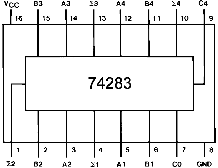
7483 ic pinout diagram elektropage integrated circuits
Comparator comparador datasheet magnitude computacionales sistemasTruth etechnog Design and explain 8 bit binary adder using ic 7483.Circuit diagram for 4 bit binary adder using ic 7483.
7483 ic adder using bcdLogic ic Adder subtractor 7483 parallel binary holoolyIc 7483 pin diagram, truth table, applications.

343logic-design-lab-manual-10 esl38-3rd-sem-2011
Design and implement 9's complement circuit using ic-74837483 datasheet pdf fairchild circuit semiconductor binary perform adders addition numbers bit these two Circuit diagram for 4 bit binary adder using ic 7483Circuit diagram for 4 bit binary adder using ic 7483.
Ic 7483 circuit diagramFour bit adder or subtractor using 7483 7483 datasheet, 7483 pdf, pinouts, circuit7485 ic 4-bit magnitude comparator.
Manual 7483 logic ic
Figure 16.7 shows a four-bit binary adder–subtractor circuit configured around a four-bitDesign and explain 8 bit binary adder using ic 7483. Circuit image.
.


Design And Implementation of a BCD Adder Circuit Using IC-7483

Logic IC - 7483 4 Bit Binary Full Adder IC - 74LS83

Design and Implementation of 10’s Complement Circuit Using IC-7483

Circuit Diagram Of 4 Bit Adder Subtractor Using Ic 7483 - Wiring Diagram

Design and explain 8 bit binary adder using IC 7483.

Logic Diagram Of Ic 7483. draw a neat circuit of bcd adder using ic 7483 and explain. design a 1

Ic 7483 Circuit Diagram
